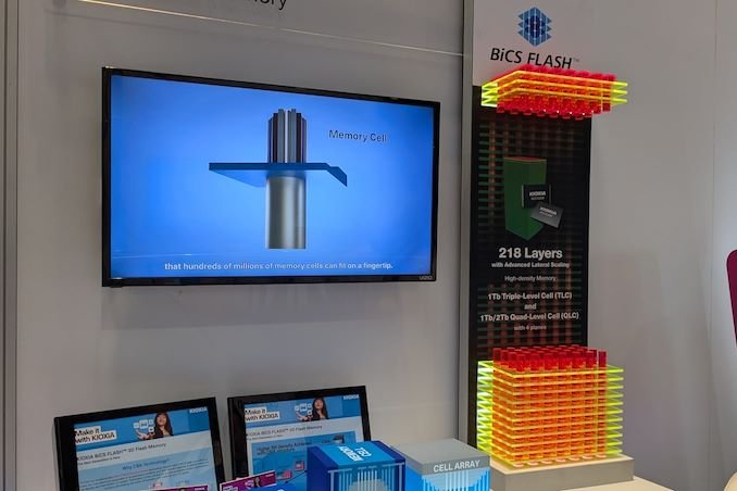
218 Layers With Superior Scaling
Kioxia’s booth at FMS 2024 was very busy, with multiple technology demonstrations keeping visitors busy. The overview of the BiCS 8 manufacturing process first caught my attention. Kioxia and Western Digital declare BiCS 8 will be sampled in March 2023. 2Tb QLC NAND device and Coverage Western Digital’s 128 TB QLC enterprise SSD proof-of-concept demonstration. At the Kioxia booth, we got more insights.
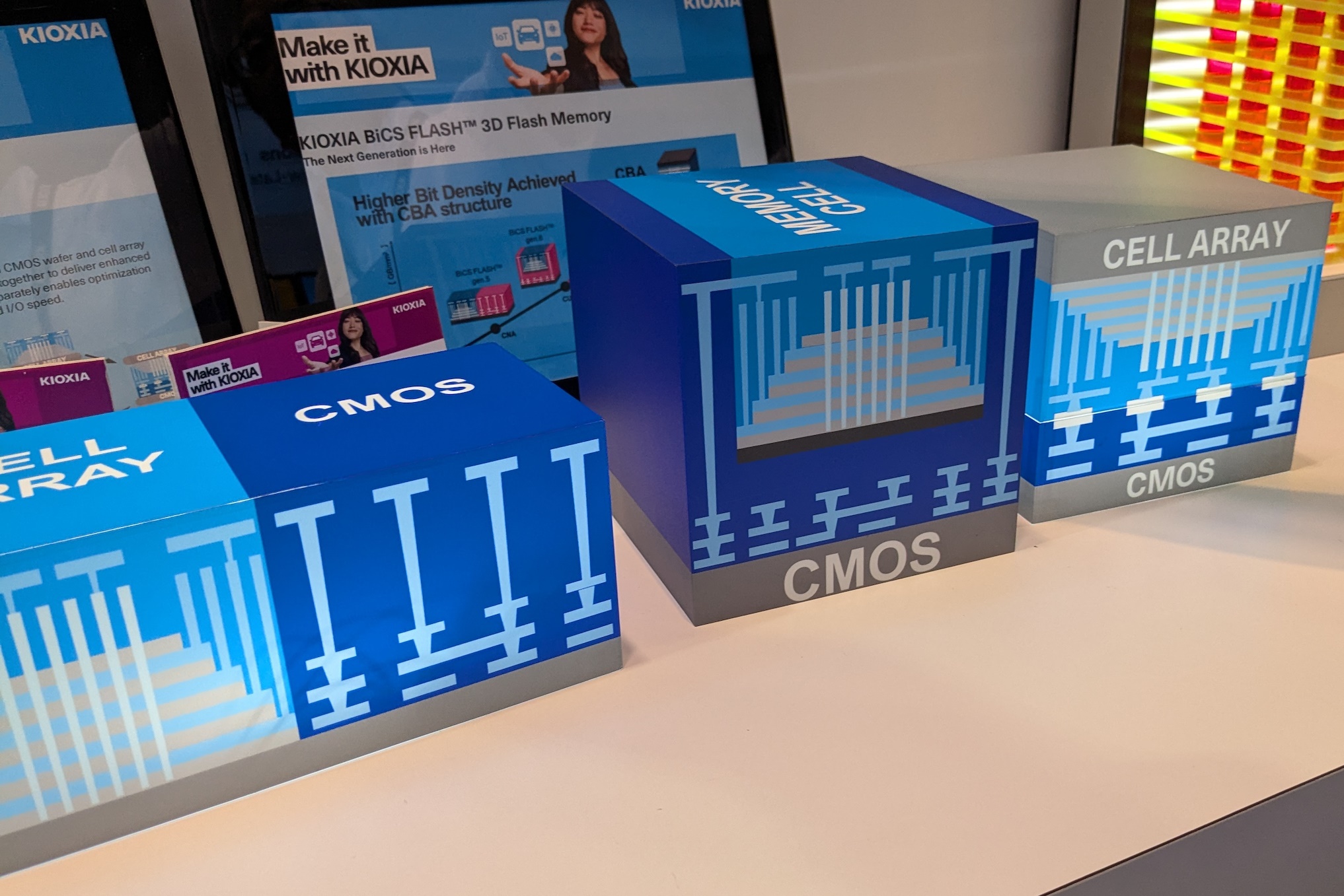
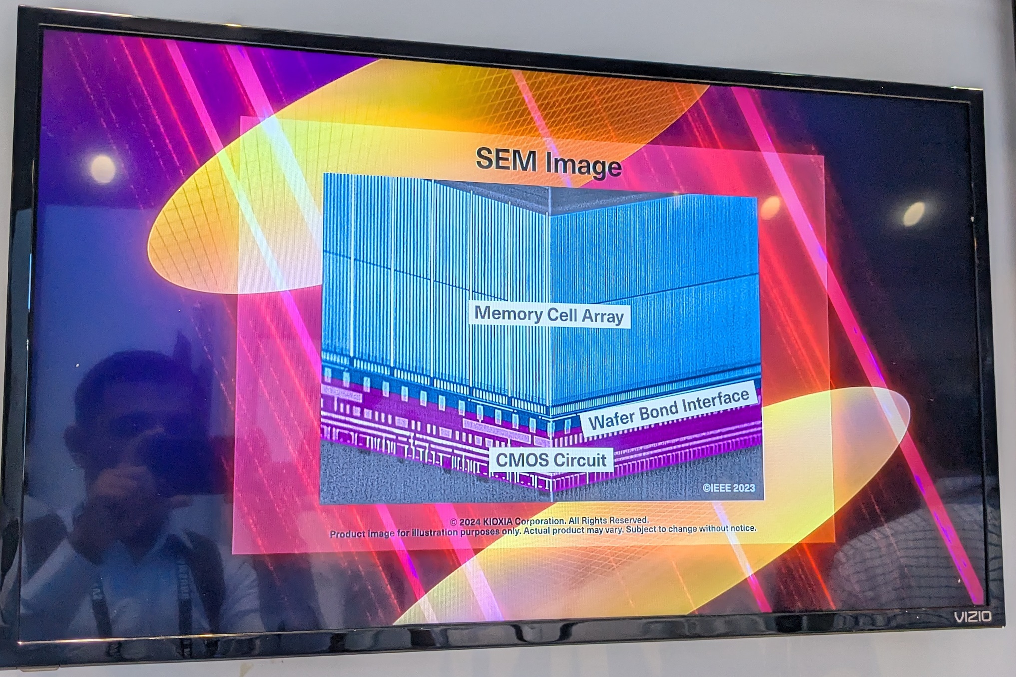
Traditionally, the fabrication of flash memory chips involves placing associated logic circuitry on the periphery of the flash memory array (CMOS process). The process then continues with placing the CMOS underneath the cell array, but the wafer development process is sequential, first making the CMOS logic and then placing the cell array on top. However, this presents some challenges, as the cell array requires high-temperature processing steps to ensure higher reliability, which may be detrimental to the health of the CMOS logic. Thanks to recent advances in wafer bonding technology, the new CBA process allows CMOS wafers and cell array wafers to be processed independently in parallel and then spliced together, as shown in the model above.
BiCS 8 3D NAND contains 218 layers, while BiCS 5 has 112 layers and BiCS 6 has 162 layers. This generation retains the four-planar charge trap structure of BiCS 6. The QLC version is available in two capacities – 1 Tbit and 2 Tbit.
Kioxia also noted that while the layer count (218) doesn’t compare favorably to the latest from competitors, its scale-out/cell shrink gives it in-place density and operating speed (3,200 metric tons/second). For reference, Micron’s latest NAND launch – G9 – With 276 layers, bit density in TLC mode is 21 Gbit/mm2operating speed up to 3600 MT/s. However, its 232L NAND only operates at speeds up to 2400 MT/s and has a bit density of 14.6 Gbit/mm2.
It must be noted that the CBA hybrid bonding process has advantages over processes currently used by other suppliers, including Micron’s CMOS Under Array (CuA) and SK Hynix’s 4D PUC (Peripheral Under Chip) developed in the late 2010s. It is expected that other NAND suppliers will eventually move to some variation of the hybrid bonding scheme used by Kioxia.
2024-08-12 14:00:00