
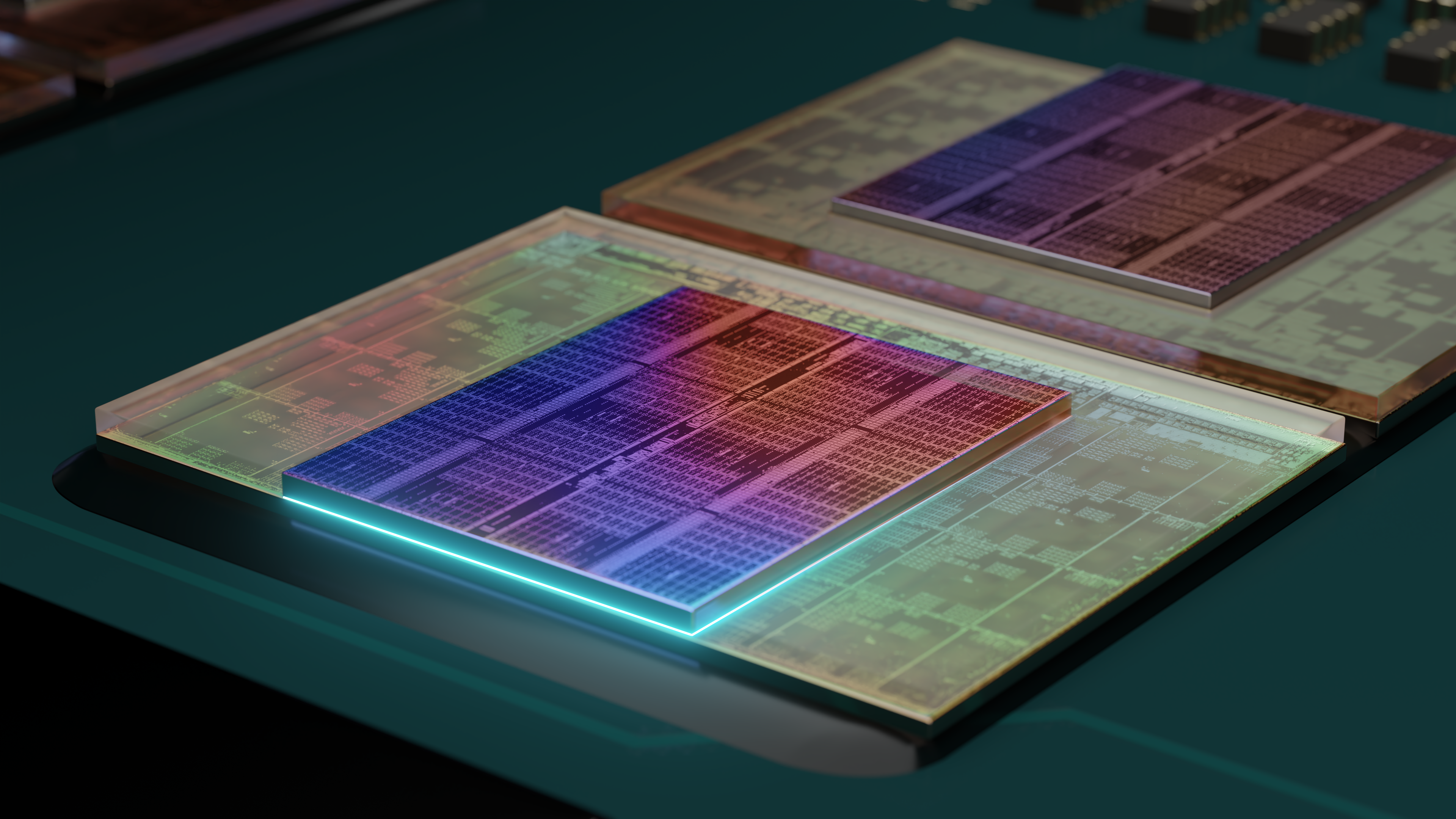
It’s been over a month since AMD launched its Ryzen 7 9800X3D processor, and the processor has quickly established itself Fastest gaming CPU in the world. Investigating AMD’s design philosophy, semiconductor analyst Tom Wasik (via Hardware luxury) has taken apart the die, and his first reported results indicate that a large portion of the Ryzen 7 9800X3D is simply dummy silicon for structural integrity. Still, AMD squeezed a ton of performance out of its second-generation 3D V-Cache design, earning a solid victory over the competition with Intel’s Arrow Lake chips.
Ryzen 9000 X3D processor is structured Place the L3 SRAM cache chip under the heat-generating CCD (an arithmetic chip with eight CPU cores). Although AMD has never elaborated on the specifics of its stacking approach, it could achieve higher clock speeds by providing more thermal headroom. The report mentioned that both CCD and 3D V-Cache wafers are thinned to below 10μm level to expose TSV for hybrid bonding. Combined with the BEOL (back end of line) (the part with the metal layers required for connections), the total thickness of the SRAM and CCD packages is 40-45μm.
SRAM wafers have always been a fraction of the size of computing wafers; the Ryzen 7000 3D V-Cache chip measures 36 mm2, compared to 66.3 mm2 for CCD. Tom Wassick’s research results show that the four sides of the SRAM wafer are actually 50μm larger than the CCD. In reality, a large portion of this die should be empty, but we’re still waiting for more details.
Excluding interconnects, the combined thickness of SRAM and CCD should be less than 20μm. To accommodate such a small and fragile component, AMD added a massive layer of dummy silicon on the top and bottom to ensure structural integrity. The thickness of the entire package is approximately 800μm. After subtracting the 50μm wafer stack (CCD, SRAM and BEOL), the top structural support size is 750μm. In other words, 93% of the entire stack contains only dummy silicon to keep the die intact.
The different layers are connected by an oxide coating between them. The bonding layer between the core CCD and SRAM is reportedly thinner than the bonding layer between the dummy silicon and the two dies to achieve better thermal performance.
There are still several open questions, which Tom Wasik plans to address with the help of scanning electron microscopy in future follow-up projects. Although the gaming throne has been taken away by AMD, Intel has no plans to compete with AMD’s 3D V-Cache technology, at least not yet. mainstream market. Nonetheless, we expect AMD to release the 12-core and 16-core Ryzen 9 9900X3D and Ryzen 9 9950X3D International Consumer Electronics Show next month.