
Nvidia’s Blackwell GPU is one of the most complex semiconductor devices ever created, significantly increasing the difficulty of manufacturing, packaging and testing. according to British Financial Times, Advantest CEO Doug Lefever said testing takes three to four times longer Blackwell Data Center GPU Compare this to Hopper Data Center GPUs, as each unit must be tested dozens of times on different tools before shipping.
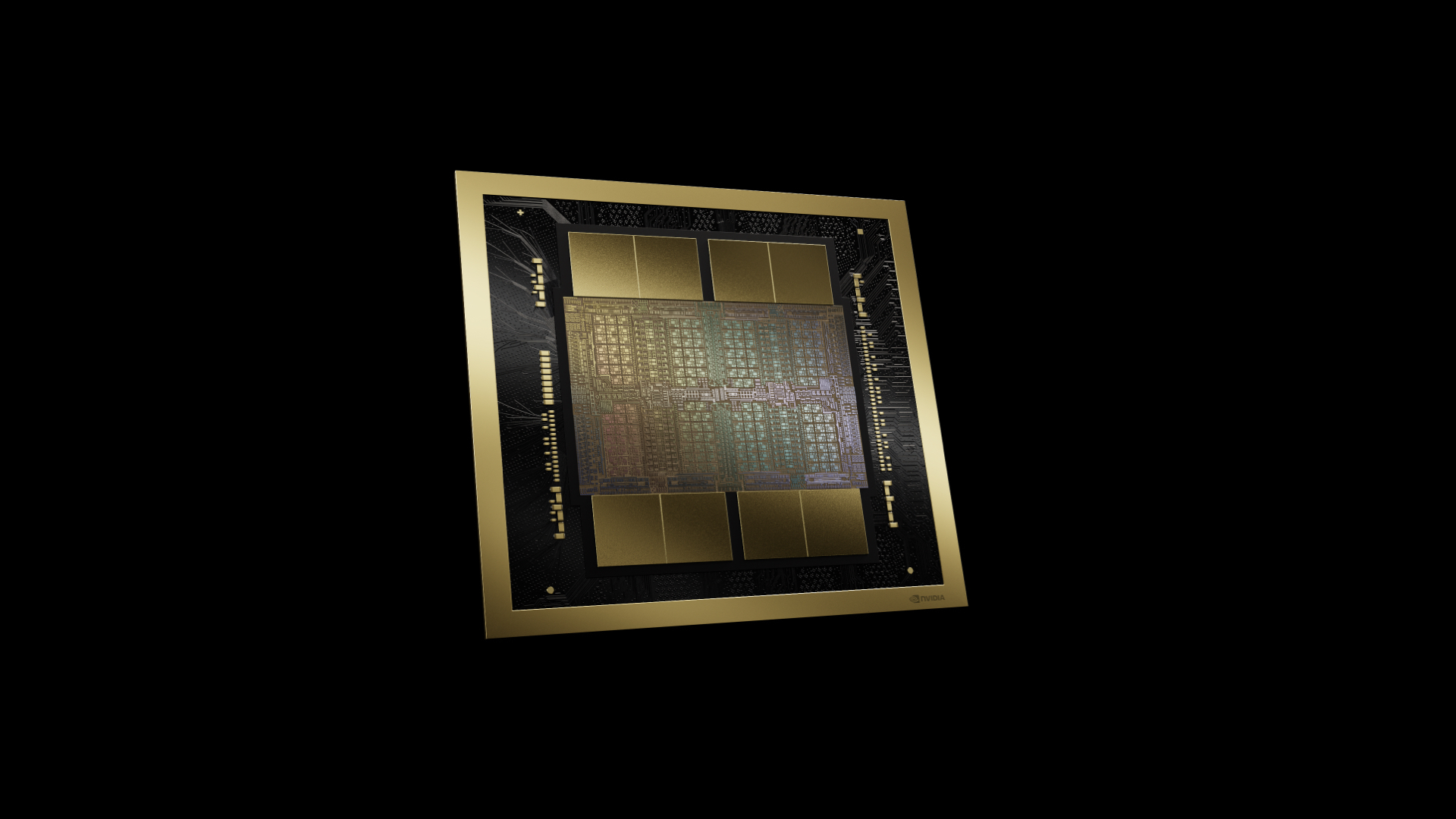
Nvidia Blackwell B100/B200 The GPU consists of two computing chipsets containing 104 billion transistors and 8 HBM3E memory chipsets, which are interconnected through the following interfaces: TSMC’s CoWoS-L packaging technology. This is in stark contrast to Nvidia’s Hopper H100 GPU, with one 80 billion transistor die and 6 HBM3 memory stacks.
Typically, as the number of transistors increases, test complexity increases almost exponentially because the wafers require more test patterns and longer test times. Test protocols must cover high-speed interconnects, stress conditions, thermal conditions (extreme for the B200) and multiple operating modes (Blackwell has added FP4 support). Since Blackwell involves two highly complex small dies with new features and higher thermal performance, the time to test them will naturally more than triple.
There’s more to this. TSMC’s CoWoS-L 2.5D packaging technology introduces additional testing steps (sometimes multiple testing stages) to ensure that every component in the package is functioning properly and the interconnect is reliable.
With Blackwell, one has to test compute dielets and memory dielets separately (although DRAM manufacturers test HBM3 stacks), and then test the GPU multiple times when adding those dielets to their RDL interposers. We don’t know the exact number of times Nvidia’s Blackwell B100 and B200 GPUs and modules are tested during the packaging and assembly process. Still, these GPUs have gone through more testing iterations than the Hopper H100 GPUs.
Overall, Blackwell’s longer test times reflect the increasing complexity of these AI and HPC GPUs and the need for extensive validation to ensure performance across a variety of data when running with other components such as CPUs, DPUs, and network interface cards. Performance and reliability in a central environment.