MIT’s Photonic Chip Approach to Hyper-Efficient AI Computation
eWEEK content and product recommendations are editorially independent. We may earn money when you click on our partners’ links. learn more.
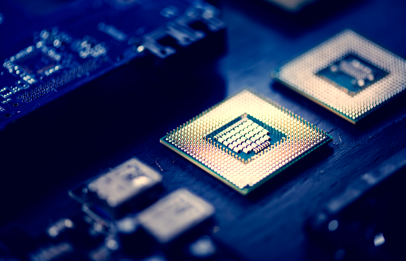
The Massachusetts Institute of Technology (MIT) has taken a big step in the field of artificial intelligence with the launch of a photonic chip that promises faster, more energy-efficient artificial intelligence computing. Developed by MIT researchers, this cutting-edge technology achieves an impressive 96% accuracy during training and 92% accuracy during inference, matching the performance of traditional electronic processors Comparable, while power consumption is significantly reduced.
The chip can complete key operations in half a nanosecond, which could pave the way for ultra-high-speed computing Artificial intelligence applications. This innovation solves a growing problem in the field of artificial intelligence: the increasing energy requirements of traditional electronic hardware.
Why photonic chips are important
The need for more efficiency AI model training Deep neural networks (DNN), the backbone of modern artificial intelligence, are constantly evolving as they require massive computational resources. It is difficult for traditional electronic hardware to keep up with these demands. Consume huge amounts of energy and approaching its performance limits. Photonic chips developed at MIT could change that, performing critical calculations at lightning speed, completing tasks in less than half a nanosecond.
deep neural network Data is processed through interconnected layers, mimicking the human brain. They rely on two main types of operations: linear calculations involving matrix multiplication and nonlinear calculations that allow the model to detect complex patterns. While photonic processors have previously been able to manage linear tasks, the challenge has always been nonlinear calculations because light particles (photons) naturally resist interacting with each other.
“Nonlinearities in optics are very challenging because photons don’t interact easily with each other,” explains Saumil Bandyopadhyay, a visiting scientist at MIT who participated in the study. The project. “This makes triggering optical nonlinearity very power-hungry, so building a system that can do this in a scalable way becomes very challenging,”
Solve non-linear puzzles
An MIT team led by Dirk Englund of the Quantum Photonics and Artificial Intelligence Group met this challenge by designing a “nonlinear optical functional unit” (NOFU). The researchers “constructed an optical deep neural network on a photonic chip using a three-layer device that performs linear and nonlinear operations,” the report said.
These hybrid devices integrate photonic and electronic components to handle nonlinear operations. By converting small amounts of light into electrical current, the chip eliminates the need for power-hungry amplifiers, thus maintaining energy efficiency. The researchers successfully manufactured test wafers using the same casting process as traditional CMOS wafers. This scalability means photonic wafers can be integrated into existing manufacturing systems, paving the way for widespread adoption in the near future.
As artificial intelligence computing becomes increasingly integrated into applications such as self-driving cars, natural language processing, and advanced robotics, innovations like MIT’s photonic chip promise to revolutionize the field by making artificial intelligence faster and greener.
This research, funded by the National Science Foundation, the U.S. Air Force Office of Scientific Research, and NTT Research, will lay the foundation for the next generation of artificial intelligence hardware.
explore Top companies pushing the boundaries of artificial intelligence and redefining how the technology is used across industries.
2024-12-20 12:04:00