Mystery solved as report tells us which chip powers Huawei’s Mate 70 series

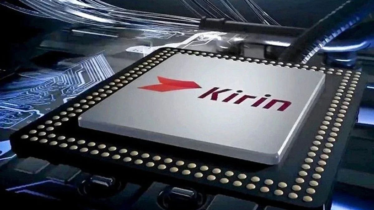
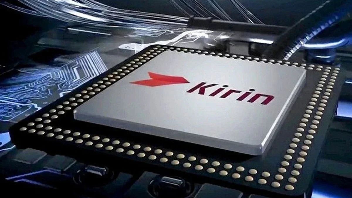
TechInsights did say that it found changes to the Kirin 9020’s circuit floor plan that enhance the performance and efficiency of the new chip. The chip size of Kirin 9020 is 15% larger than that of Kirin 9010.
“The Kirin 9020 processor is not a major redesign, but an incremental improvement over its predecessor, the Kirin 9010. This approach demonstrates HiSilicon’s focus on improving existing designs while leveraging SMIC’s capabilities in advanced semiconductor manufacturing .
TechInsight’s findings suggest that Huawei and SMIC will have difficulty following up on last year’s shock launch of the Mate 60 series, which featured 5G-capable Kirin chips for the first time since 2020’s Mate 40 series. The United States changed its export rules in 2020, banning foundries that use American equipment to produce chips from shipping advanced silicon to Huawei.
According to TechInsights, Huawei Mate 70 Pro+ is powered by the 7nm Kirin 9020. |Image source-Huawei
Qualcomm secured a license that allows the San Diego-based chipmaker to supply Snapdragon APs to the Huawei P50, Mate 50 and P60 flagship series. Qualcomm received a license from the U.S. Commerce Department because it tweaked the chip so that it would not work with 5G airwaves. The United States has been trying to prevent the Chinese military from acquiring advanced chips, including those that support 5G.
At the same time, the U.S. and Dutch governments are blocking Chinese companies from obtaining the extreme ultraviolet lithography machines needed by foundries to produce chip sets at 6 nanometer nodes and below. In short, lower process nodes usually mean using smaller transistors. This allows wafers to have higher transistor count (the number of transistors within the wafer) and higher transistor density (the number of transistors packed into a specific area of the wafer). The more transistors a chip has, the more powerful and efficient the chip is usually.
2024-12-11 21:07:04