
While Nvidia GeForce RTX 5090 Founders Edition The graphics card features the world’s most powerful consumer GPU released to date, as well as one of the most power-hungry GPUs ever created. As a result, Nvidia needed an entirely new PCB, so it came up with a three-piece design that is unlike anything we’ve seen before. The main board houses the GB202 chip, memory, and a monster 30-phase voltage regulation module (VRM).
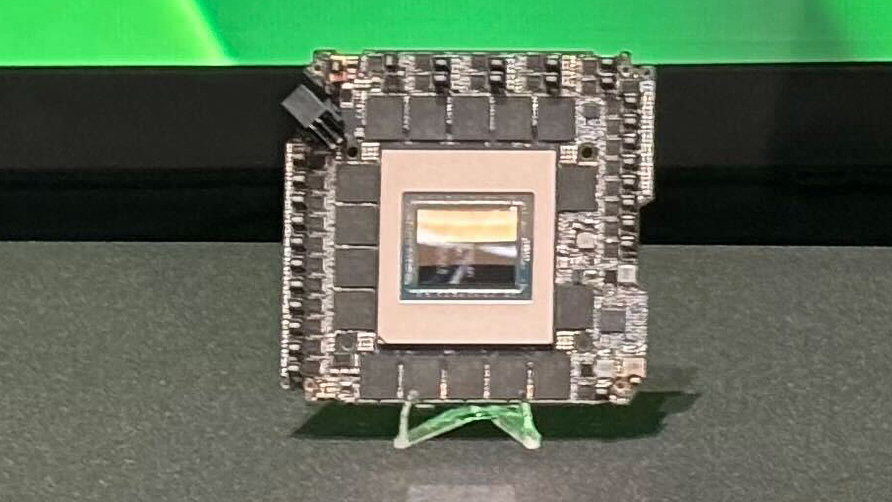
Nvidia says the GeForce RTX 5090 Founders Edition, which promises to be best video carduses a “unique three-piece printed circuit board”. On your own KES At the 2025 presentation, the company showed off only a “high-density” PCB containing a massive GB202 GPU with 92 billion transistors, accompanied by 32GB of GDDR7 memory connected via a 512-bit interface to the GPU.
While the new GeForce RTX 5090 FE has massive processing power, its “main” PCB is really small compared to the GeForce RTX 4090 (pictured below). To get an idea of how big or small the new model is, take a look at the size of the memory chips (they come in 14 x 12mm packs) and compare its size to the previous generation product that included memory packs. exactly the same sizes. There is also a picture of the old version below.
The card has a single 12V-2×6 power connector, providing up to 55A of current to power up to 600W graphics cards over the 12V auxiliary rail. It also has a powerful 30-phase power delivery design (vs. 23-phase VRM on GeForce RTX 4090 Founders Edition). Considering that the Nvidia GeForce RTX 5090 is rated at 575W total board power (TBP), the use of a massive 30-phase VRM is justified since the GPU and memory require a lot of stable, clean power without spikes and drops to function properly. . Moreover, a more complex power design can improve the performance of the product. However, we can only guess how much overclocking headroom these GeForce RTX 5090 boards will have with a single 12V-2×6 power connector.
The board lacks display outputs, power headers for fans, and PCIe mesh, although there are additional headers on the rear panel. Therefore, we assume that the GeForce RTX 5090 Founders Edition card has two more boards that are not yet shown. We can only speculate as to why Nvidia separated the display outputs, PCIe meshes, and fan headers from the main board.
One reason could be that each PCB was designed with a specific purpose, providing cleaner signal routing and more efficient use of space. Additionally, separating display outputs, PCIe, and fan headers can minimize electrical noise and improve GPU power supply stability.
Nvidia could also take a page from its own book with the GeForce 8800 GTX/Ultra (G80 GPU) and separate the display engines from the GB202 GPU to save precious silicon compute space and optimize the overall GPU design. Perhaps this will allow Nvidia to offer different GB202 products by mixing and matching plug-ins. For example, a GB202-based card installed in a server does not require display output, whereas some OEMs may offer a different display output configuration to their customers.
Above we see a larger older PCB. While the new GeForce RTX 5090 FE has massive processing power, its “main” PCB is a very small card compared to the GeForce RTX 4090.
It’s interesting to note that Nvidia’s partners will continue to use single-board designs for the GeForce RTX 5090 graphics cards. Thus, the unique three-piece PCB is not a requirement for Blackwell’s flagship graphics cards, but rather a thoughtful design decision by Nvidia engineers, who had their own reasons for using such unorthodox design.