
Take a quick look successful start The installation of ASML’s Twinscan NXE:3800E EUV lithography system at its Innovative Integrated Manufacturing (IIM-1) facility in Chitose, Hokkaido, marks an important milestone for Japan’s semiconductor industry. By 2025, the tool will be used 2nm process technology Then commercial semiconductor production begins 2027.
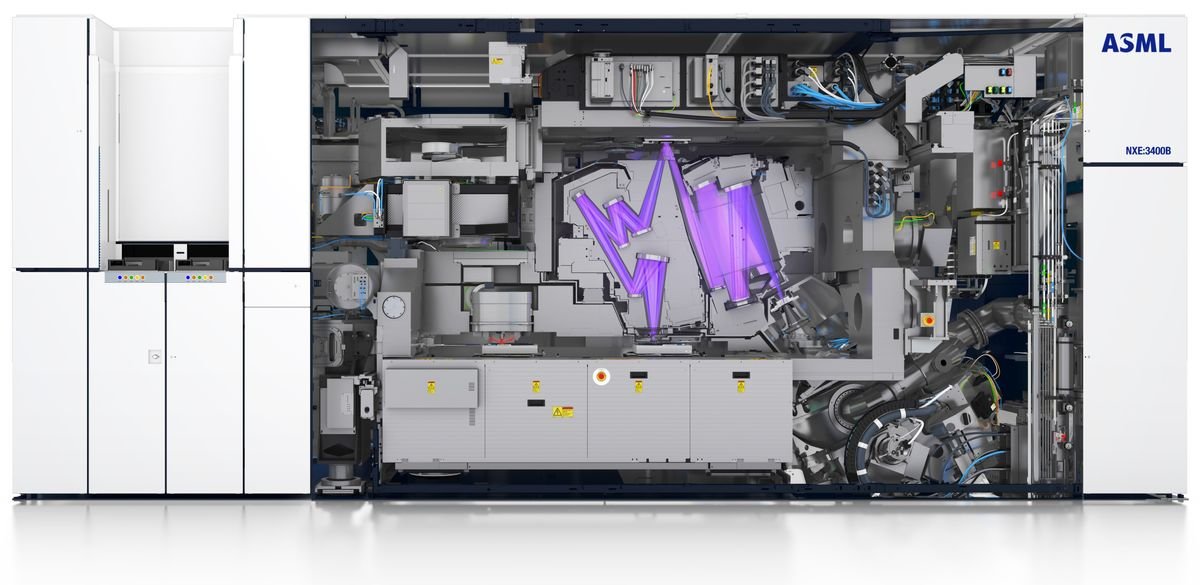
ASML’s Twinscan NXE:3800E lithography system is the company’s most advanced lithography tool currently, specifically designed to produce wafers using 2nm and above process technologies. Equipped with ASML’s latest high-power light source, a new wafer handler, a faster wafer stage and other components needed to support increased throughput, the machine is capable of processing more than 220 wafers per hour at a dose of 30 mJ/cm² performance.
The system weighs 71 tonnes, is 3.4 meters high and had to be assembled in four stages. Rapidus expects to complete the installation by the end of this month (according to Nikkei Index) and set a new milestone for Japan’s semiconductor industry as it is the country’s first EUV machine designed to produce logic wafers using EUV-based process technology.
Rapidus’ IIM-1 facility will begin trial operations in April 2025. The working principle and adjust the manufacturing process accordingly. As a result, lower defect densities will be achieved faster (thus increasing test wafer yield).
Rapidus has partnered with International Business Machines Corporation Developing 2-nanometer process technology for logic chips that rely on full-gate transistors. The company hopes to start mass production of 2nm semiconductors in 2027, which is 1.5-2 years behind Intel and TSMC, which plan to start commercial production of 1.6nm and 2nm class wafers in the second half of 2025. It is a breakthrough for businessmen, but it will be a major breakthrough for the Japanese semiconductor industry.
Rapidus also plans to provide its customers with the “secret sauce” of advanced chip packaging services. First, Rapidus will package the wafers in the same factories where they are produced. Secondly, Rapidus aims to Automated chip packagingthereby shortening the cycle time. Compared with the highly automated front-end photolithography process, back-end production is still labor-intensive. While this reliance on manual work allows for some adaptability, it also limits the speed of production.
Existing advanced packaging facilities are also not yet fully automated. By introducing automation at this stage, Rapidus aims to significantly increase the efficiency and speed of chip packaging, which it hopes will be a critical improvement as advanced packaging technologies become more complex. In addition, the company is working closely with a number of Japanese suppliers to purchase materials required for back-end operations, which will promote the development of the local semiconductor industry.
Rapidus’ Integrated Innovative Manufacturing (IIM-1) facility will cost about $32 billion when fully built and equipped, but the company still must secure funding. Japanese banks are reluctant to provide funds to companies without a track record.