Just days before Christmas, the U.S. government finalized financing deals with three companies: Samsung, Ankor and Texas Instruments. The two companies will build a leading 2nm wafer fab, an advanced packaging facility, and three large-scale analog and embedded chip fabs, which will produce tens of millions of ICs every day.
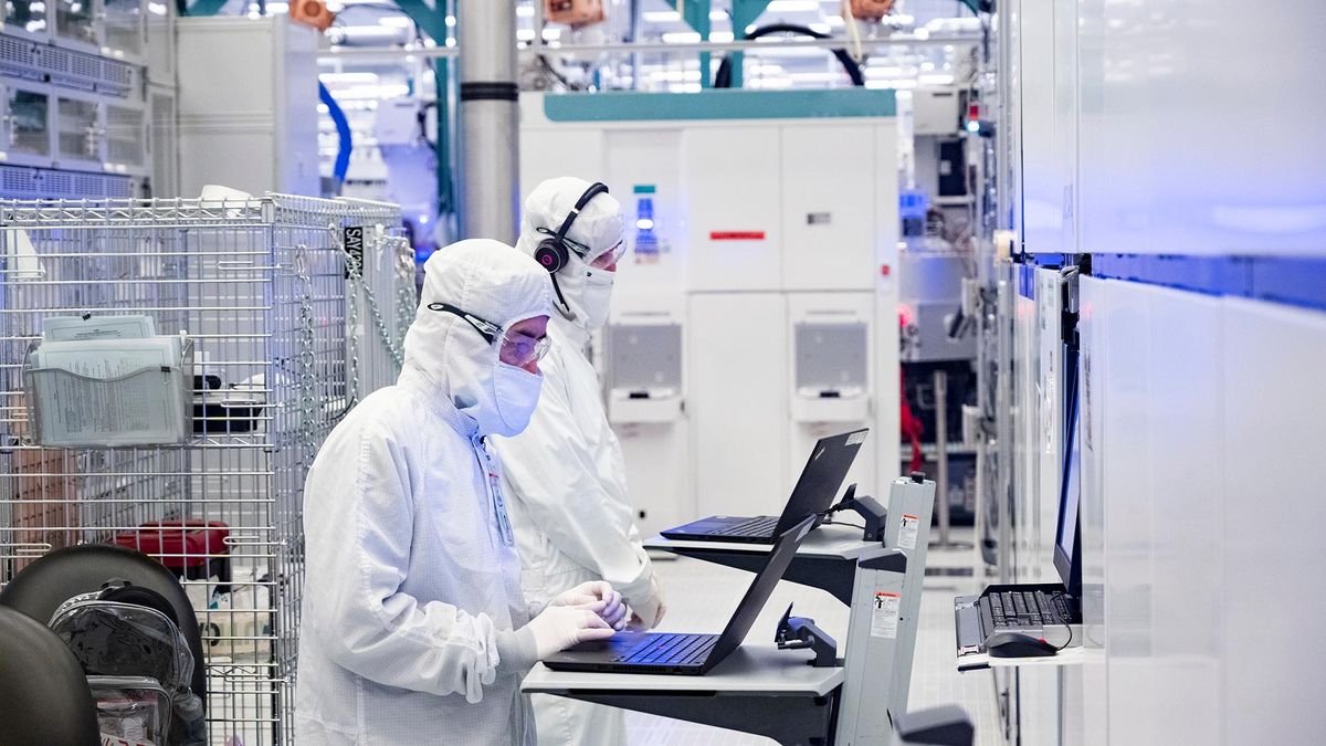
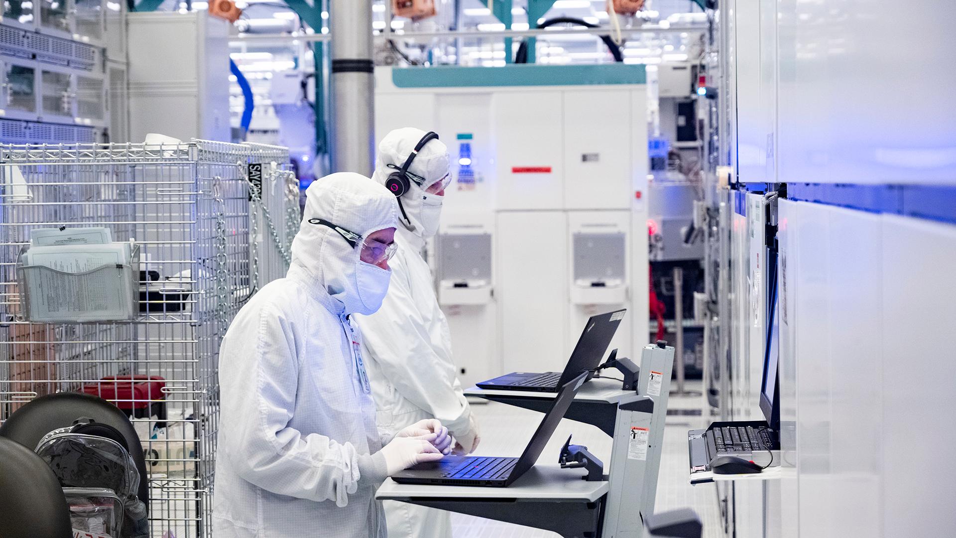
Samsung 2nm enters the United States
The U.S. government has approved the most US$4.745 billion Funding for Samsung under the Chip and Science Act. While Samsung’s foundries have every reason to celebrate, it’s important to point out that the allocation is $1.65 billion lower than the amount originally announced in April, likely due to Samsung itself cutting $30 from its investment plans due to an overall reconsideration. billion dollar results.
U.S. government investment will support Samsung no matter what $37 billion project Construction of a two-phase state-of-the-art wafer fab in Tyler, Texas, adjacent to R&D facilities, to begin production of fully depleted silicon-on-insulator (FD-SOI) process technology for aerospace, automotive and defense applications The chip project is expected to be completed in 2030 and all manufacturing capabilities will be put into operation.
The two-stage fab will be able to produce chips using Samsung’s 2nm-level process technology, although the company did not disclose which nodes this means. The company’s SF2 node was rebranded as SF3P process technology, and its successors – SF2P (enhanced performance), SF2X (node for CPU and HPC) and SF2Z (2nm class with backside power) – are considered true The distance between the 2nm nodes was originally 2nm.
In addition to the two factories, Samsung will establish a dedicated research and development manufacturing facility dedicated to researching manufacturing process technologies that are several generations advanced than those currently produced. To ensure fab developers, engineers and fab workers are comfortable with and involved in the development of next-generation tools, the R&D facility will also feature dedicated space for early collaboration with fab equipment suppliers. In addition, Samsung will be able to work with partners to develop new materials such as ultrapure gases and resists.
Finally, Samsung’s project includes expanding its wafer fab in Austin, Texas, to utilize its FD-SOI process technology to manufacture chips in the US aerospace, automotive and defense sectors. Wafers are made from wafers.
The construction phase of the projects is expected to create more than 17,000 jobs and add 4,500 permanent manufacturing jobs over five years.
Amkor to receive $407 million to build advanced packaging facility
The Biden-Harris administration will also provide $407 million in direct funding to Amkor, a leading outsourced semiconductor packaging and test (OSAT) company, to establish a US$1.7 billion (from Initially expected to be US$2 billion) state-of-the-art packaging facility in Peoria, Arizona.
The new facility covers an area of 55 acres and has more than 500,000 square feet of clean room space to support a variety of packaging solutions including traditional, 2.5D and 3D technologies. The factory will be operational by the end of 2027 and will primarily serve TSMC’s customers due to its proximity to TSMC’s Fab 21 in Arizona. Apple will become Amkor’s major customer in the United States.
Texas Instruments: A large number of fabs
Texas Instruments has received up to $1.6 billion in CHIPS Act funding and expects to receive $8 billion in tax credits to expand semiconductor manufacturing in Texas and Utah.
The funds will be used to equip the first Sherman Phase 1 clean room, build the second Phase 2 enclosure and upgrade the Lehi facility with advanced logic tools. The facilities will produce analog and embedded wafers on specialized 28nm to 130nm production nodes for devices such as automotive and medical devices. The measure is expected to create more than 2,000 direct jobs at TI and thousands more in construction and related industries.