- SK Hynix’s 321-layer NAND targets artificial intelligence-driven data storage needs
- 321-layer NAND flash memory, data transfer speed increased by 12%
- AI storage needs drive innovation in large-capacity NAND solutions
Samsung The head-to-head competition with SK Hynix in the NAND flash memory market continues, with the latter taking the lead with the launch of new products.
SK Hynix, the world’s second-largest memory chip manufacturer, recently became the first company to mass-produce more than 300 layers of triple-level cell (TLC) NAND flash memory.
The company’s recently launched new 321-layer, 1-terabit TLC 4D NAND flash memory will revolutionize the data storage industry, paving the way for more affordable ultra-high-capacity solid-state drives (solid state drive) capacity exceeds 100TB.
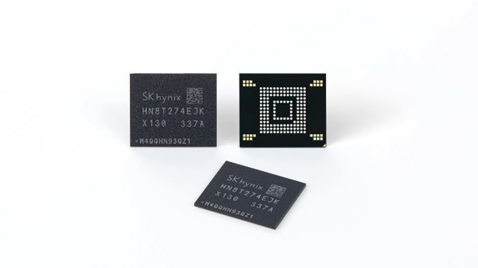
SK Hynix 321-layer NAND
The NAND industry is racing to push the limits of data storage technology, and SK Hynix’s achievement is an important milestone.
Following the launch of 238-layer NAND flash memory last year, SK Hynix’s latest 321-layer NAND flash memory has set a new industry standard. The company plans to start supplying these chips to customers in the first half of 2025, targeting the booming artificial intelligence (artificial intelligence)AI) market requires high-efficiency, energy-saving storage solutions.
321-layer NAND is achieved through SK Hynix’s “three-plug” process technology, which involves electrically connecting three plugs through optimized subsequent steps, thereby significantly improving the speed, power efficiency and overall performance of the chip.
SK hynix has also developed a low-stress material and introduced technology to automatically correct the alignment between plugs to further optimize the manufacturing process.
Compared with the previous 238-layer NAND, the data transfer speed of the 321-layer product has increased by 12%, and the read performance has increased by 13%. In addition, it can reduce power consumption by more than 10%. SK Hynix’s new NAND increases productivity by 59%, providing enhanced storage solutions for AI data centers and device-side AI applications.
While SK Hynix achieved this historic feat, its main rival Samsung is not far behind. Samsung is 400-layer NAND flash memory chips reportedly under developmentscheduled for release in 2026.
The company’s roadmap includes the development of bonded vertical NAND (BV NAND) technology that will enable greater storage density and minimize heat build-up. Samsung’s long-term goal is to launch NAND chips with more than 1,000 layers by 2030, potentially breaking the 200TB storage barrier for AI-driven SSDs.
Jungdal Choi, head of NAND development at SK Hynix, said: “SK Hynix has added a perfect product portfolio in the ultra-high-performance NAND field on top of the DRAM business led by HBM, and is expected to become one of the full-stack AI memory providers.”
through Kaidi Global